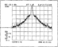
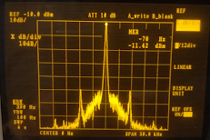
After full recapping of the PSU and CRT modules of my R3361B the instrument began showing a pronounced vertical instability: looking at the CAL signal (30MHz / -20dBm) the trace was randomly jumping up and down in a 5-8 dB range.
I initially suspected a side effect of my recent recappings, but that was not the case.
Long story short:
during recapping I was forced to move/dismount/rotate/drag the unit multiple times..
In one of these movements I had to drag the instrument towards me:
the two front feet inadvertently went over the edge of the table; it has
been as if the instrument had fallen from a height of 2/3 cm hitting the table edge right on its bottom front part.
This has been the actual moment since the instability began to show up.
Stated that:
- the input LPF-coupler assembly is located just behind the input socket in the right bottom front part of the unit - just where it took the hit;
- the LPF (THP118) and the coupler (THP202) are each built as gold stripes laid down on a ceramic substrate; the two parts are connected via a very thin solder joint crossing between the two ceramic wafers..
I decided opening the RF input section , and....
BINGO!
the solder joint in my unit had flown off as you can see from this picture:
The unjoi"ned" joint |
Here is the block diagram of the involved parts (the failed joint circled in red):
The problem was now how to fix it without significantly affecting the features of the instrument.
Doubts were about:
- the surface to solder is less then a couple of mm2;
- the material to be soldered is a thin layer of gold laid down on a ceramic
support from which it can easily lift up by the effect of heat;
- the part is a VERY sensitive part and very high frequencies are involved there and so the geometry of the traces counts A LOT;
- Is it advisable to use some solder flux here??
- Is it advisable to put a very thin copper strand between the parts?
- how can we avoid the solder from spreading too much along the traces? (the gold plated traces transport tin very easily).
Here is an excerpt of the suggestions I've got from the eevblog forum:
- solder a thin copper strand between parts is OK and avisable;
- put kapton / polyimide tape on the areas that you don't want to have solder on;
- conservative tip heat setting, just enough to melt the solder and not much more;
- use hot air from the underside to pre-heat (evenly !) and then solder very carefully (unfeasible here as per hardware setup..);
- take your time; it is a repair where you can easily mess up it all;
- No lead free solder within 100 miles of this project!
- Paste flux, minimal quantity (speck on end of a toothpick)
With these suggestions in mind I proceeded against the unknown and started the procedure depicted by the following pictures:
..masking |
..soldering |
Finish!! |
I didn't put any copper strand (too difficult in a so small fixture).
Final cosmetic result is not as good as I would have liked it to be; I had to use
400°C to get a good bright joint: it was like as the ceramic substrate
was sinking a lot of heat. Due to lack of heat the solder lumped instead
of spreading as expected.
I any case the S.A. is now stable again.
I should now check it for flatness on the entire frequency range but I
do not have any suitable sig-gen... (I only have an HP8640B-no
doubler..).
May be I can perform some test using the internal tracking generator.. will see.
For the frequency ranges I usually work on (< 0,5GHz) I believe this can be considered a success.
Conclusion:
Advantest
spectrum analyzers must be treated like very fragile crystal glasses,
absolutely preventing sharp hits, even if not very violent.
Hope this can help someone else with similar problem.
Emanuele.
NOTE: Someone drew my attention to the left side of the solder where a crack in the ceramic wafer is quite clearly visible; this is something I will address in the future. At the moment I don't see any problems in the functionality of my SA.